EMICRO Parte I (FEEVALE, Novo Hamburgo)
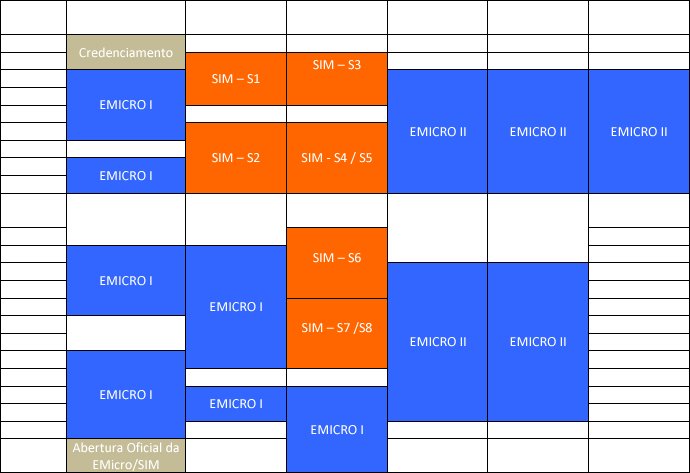
Segunda de manhã (25/04)
9:00- B0 - Introdução - Alexandro Girardi (UniPampa)
9:15- B1 -Tecnologia MOS (TBD)
10:05- B2 - Projeto Físico de Portas Lógicas e Redes de Transistores - Paulo Butzen (UFPel)
10:55 - intervalo
11:15- B3 - Metodologias de Projeto Físico (Standard Cell, Sintese Automática, Blocos Regulares, Structured ASIC, FPGA) - Jose Guntzel (UFSC)
12:05 - almoço
Segunda de tarde (25/04)
13:30 - B4 - Ferramentas de CAD - Marcelo Johann (UFRGS)
14:20 - B5 - Fluxo de projeto digital (usando Cadence) - Jumir Vieira de Carvalho Junior (NSCAD)
15:10 - intervalo
15:30 - B6- Projeto de Circuitos Tolerantes a Falhas - Fernanda Kastensmidt (UFRGS)
16:20 - B7 - Teste e Projeto Visando o Teste de Circuitos e Sistemas Integrados - Marcelo Lubaszewski (UFRGS/CEITEC)
17:10- Palestra CEITEC
17:50- Abertura Oficial da EMicro/SIM
Terça de tarde (26/04)
13:30 - B8 - Fluxo de projeto Analógico - Everton Luis G. Ghignatti Jr. (NSCAD)
14:20 - B9 - Sistemas Embarcados - Lisane Brisolara (UFPel)
15:10 - B10 - Circuitos Assíncronos - Ney Calazans (PUCRS)
16:00 - intervalo
16:20 - B11 - Estudo de caso (UFSM)
16:50 - B12- Tendências - Ricardo Reis (UFRGS)
Programação SIM 2011
Terça-feira, 26/04
Sessão 1: DESIGN AUTOMATION TOOLS 1
08h30m – 08h45m
VEasy: a Functional Verification Tool Suite
Samuel Nascimento Pagliarini and Fernanda Lima Kastensmidt
08h45m – 09h00m
Gate Sizing Minimizing Delay and Power/Area
Gracieli Posser, Guilherme Flach, Gustavo Wilke and Ricardo Reis
09h00m – 09h15m
Evaluating Stimuli Generation Using the VEasy Functional Verification Tool Suite
Paulo A. Haacke, Samuel N. Pagliarini and Fernanda L. Kastensmidt
09h15m – 09h30m
Using Transistor Networks to Reduce Static Power in CMOS Circuits
Gerson Scartezzini and Ricardo Reis
09h30m – 09h45m
Transistor Sizing Analysis of Regular Fabrics
Felipe Marranghello, Vinicius Dal Bem, Francesc Moll, André Reis and Renato Ribas
09h45m – 10h00m
Computing Minimum Decision Chains of Boolean Functions
Mayler G. A. Martins, Vinicius Callegaro, Renato P. Ribas and André I. Reis
10h00m – 10h30m
Intervalo
Terça-feira, 26/04
Sessão 2: VIDEO CODING 1
10h30m – 10h45m
Multiprocessing Acceleration of H.264/AVC Motion Estimation Full Search Algorithm under CUDA Architecture
Eduarda R. Monteiro, Bruno B. Vizzotto, Cláudio M. Diniz, Bruno Zatt and Sergio Bampi
10h45m – 11h00m
Synthesis and Comparison of Low-Power Architectures for SAD Calculation
Fábio Walter and Sergio Bampi
11h00m – 11h15m
A Real Time HDTV Motion Estimation Architecture for the New MPDS Algorithm
Gustavo Sanchez, Diego Noble, Marcelo Porto, Sergio Bampi and Luciano Agostini
11h15m – 11h30m
Multilevel Data Reuse Scheme for Off-Chip Memory Accesses Reduction Applied to a Motion Estimation Architecture
Mateus Grellert, Felipe Sampaio, Julio C. B. Mattos and Luciano Agostini
11h30m – 11h45m
Fast Distortion-Based Heuristic and Hardware Design for the H.264/AVC Intra-Frame Decision
Daniel Palomino, Guilherme Corrêa, Luciano Agostini and Altamiro Susin
11h45m – 12h00m
Data Reuse Scheme for an Out-of-Order Motion and Disparity Estimation Targeting the Multiview Video Coding
Felipe Sampaio, Bruno Zatt, Sergio Bampi and Luciano Agostini
12h00m – 13h30m
Almoço
Quarta-feira, 27/04
Sessão 3: DESIGN AUTOMATION TOOLS 2
08h30m – 08h45m
Area Overhead and Performance Impact of Regular Transistor Layout Design in Digital Integrated Circuit
V. Dal Bem, P. F. Butzen, F. S. Marranghello, A. I. Reis and R. P. Ribas
08h45m – 09h00m
SET and SEU Simulation Toolkit for LabVIEW
Walter Calienes Bartra, Fernanda G. de Lima Kastensmidt and Ricardo Reis
09h00m – 09h15m
Prematurely Aborting Linear System Solver in Quadratic Placement
Guilherme Flach, Marcelo Johann and Ricardo Reis
09h15m – 09h30m
Decreasing Transistor Count Using an Edges Sharing Technique in a Graph Structure
Vinícius N. Possani, Luciano V. Agostini, Felipe S. Marques and Leomar S. da Rosa Jr.
09h30m – 09h45m
Sroute: A Router Tool for Structured ASICs
Érico de Morais Nunes and Reginaldo da Nóbrega Tavares
09h45m – 10h00m
An Algorithm for Generating Logical Expressions Using a Graph-based Approach
Julio S. Domingues Jr., Renato S. de Souza, Vinicius N. Possani, Felipe S. Marques and Leomar S. da Rosa Jr.
10h00m – 10h30m
Intervalo
Quarta-feira, 27/04
Sessão 4: VIDEO CODING 2 (em paralelo com sessão 5)
10h00m 10h15m
A Media Processing Implementation for ISDTV Middleware with Optional Hardware Acceleration Support
Jean F. G. Quadro, Tiago H. Trojahn, Juliano L. Gonçalves, Luciano V. Agostini and Leomar S. da Rosa Jr.
10h15m 10h30m
Random Search Motion Estimation Algorithm for High Definition Videos Cássio Cristani, Pargles Dall'Oglio, Diego Noble, Marcelo Porto, Luciano Agostini and Sérgio Bampi
10h30m 10h45m
CABAC Integration Into an H.264/AVC Intra-only Hardware Video Decoder
Alonso A. de A. Schmidt and Altamiro A. Susin
10h45m 11h00m
A High Throughput Hardware Solution for the H.264/AVC Quarter-Pixel Motion Estimation Refinement
Marcel Moscarelli Corrêa, Mateus Thurow Schoenknecht and Luciano Volcan Agostini
11h00m 11h15m
A Rate-Distortion Metric Targeting Perceptual Video Coding
Bruno George de Moraes, Ismael Seidel and José Luís A. Güntzel
11h15m 11h30m
Processor and Demux Integration for the SoC-SBTVD
Jeffrei Moreira, Jônatas Rech, Henrique Klein and Altamiro Susin
11h30m 13h30m
Almoço
Quarta-feira, 27/04
Sessão 5: DESIGN AUTOMATION TOOLS 3 (em paralelo com sessão 4)
10h00m 10h15m
On Placement Coloring
Guilherme Flach, Marcelo Johann, Lucas Nunes and Ricardo Reis
10h15m 10h30m
A Test Environment for Validation of Subthreshold and Leakage Current Estimation Method in CMOS Logic Gates
Kim A. Escobar, Paulo F. Butzen, André I. Reis and Renato P. Ribas
10h30m 10h45m
CAD Tool for Switch Network Profiling
Carlos E. Klock, Vinicius Callegaro, André I. Reis and Renato P. Ribas
10h45m 11h00m
A Lookup Table Method for Optimal Transistor Network Synthesis
Anderson Santos da Silva, Vinicius Callegaro, Renato P. Ribas and André I. Reis
11h30m 13h30m
Almoço
Quarta-feira, 27/04
Sessão 6: NOCS, MPSOCS AND ANALOG DESIGN
13h15m 13h30m
A Self-adaptable Distributed DFS Scheme for NoC-based MPSoCs
Thiago Raupp da Rosa, Douglas Cardoso and Fernando Moraes
13h30m 13h45m
Analog Design Methodology adopted in Training Center 1
Sandro Ferreira, Everton Ghignatti, Alcides Costa and Eric Fabris
13h45m 14h00m
Energy-efficient Cache Coherence Protocol for NoC-based MPSoCs
Tales M. Chaves and Fernando G. Moraes
14h00m 14h15m
Digital Logic Cancellation Block for a Cascade Feed-Forward Sigma-Delta Analog-to-Digital Converter
Paulo César C. de Aguirre, Felipe C. Lucchese, Lucas Teixeira, Crístian Müller and César Augusto Prior
14h15m 14h30m
Efficient Processing Element Unit for MPSoC NoC-based
Paulo Santos, Jonathan Martinelli, Cezar Reinbrecht, Débora Matos and Altamiro Susin
Quarta-feira, 27/04
Sessão 7: DIGITAL DESIGN AND EMBEDDED SYSTEMS (em paralelo com sessão 8)
14h30m 14h45m
Design and Verification of a Layer-2 Ethernet MAC Classification Engine for a Gigabit Ethernet Switch
Jorge Tonfat and Ricardo Reis
14h45m 15h00m
Functional Verification of logic modules for a Gigabit Ethernet Switch
Jorge Tonfat, Gustavo Neuberger and Ricardo Reis
15h00m 15h15m
A Direct Memory Access Controller (DMAC) IP-Core using the AMBA AXI protocol
Ilan Correa, José Luís Güntzel, Aldebaro Klautau and João Crisóstomo Costa
15h15m 15h30m
GenCode: A tool for generation of Java code from UML class models
Abilio G. Parada, Eliane Siegert and Lisane B. de Brisolara
15h30m 15h45m
Review of Localization Schemes Using Artificial Neural Networks in Wireless Sensor Networks
Stephan Hermes Chagas, Leonardo Londero de Oliveira and João Baptista S. Martins
15h45m 16h00m
Power Analysis of a Floating Point Unit for a Reconfigurable Architecture
Bruno Hecktheuer, Eduardo Nicola, Mateus Grellert and Júlio C. B. Mattos
16h00m 16h20m
Intervalo
Quarta-feira, 27/04
Sessão 8: ARITHMETIC AND DIGITAL SIGNAL PROCESSING (em paralelo com sessão 7)
14h30m 14h45m
Impact of Process Variability considering Transistor Networks Delay
Jerson Paulo Guex, Cristina Meinhardt, Ricardo Reis
14h45m 15h00m
Area and power Optimization of Radix-2 Decimation in Time (DIT) FFT Implementation Using MCM Approach Along the Stages
Sidinei Ghissoni, Eduardo Costa and Ricardo Reis
15h00m 15h15m
Development of the Overlap and Add Block for SoC-SBTVD Audio MPEG4-AAC Decoder and Hardware Interface with the wm8731 CoDec
Renê A. Benvenuti, Adriano Renner and Altamiro A. Susin
15h15m 15h30m
Cell-Based VLSI Implementations of the Add One Carry Select Adder
Jucemar Monteiro, Pedro V. Campos, José Luís Güntzel and Luciano Agostini
15h30m 15h45m
Iterative Mode Hardware Implementation of CORDIC Algorithm
Raphael A. Camponogara Viera, Paulo César C. de Aguirre, Leonardo L. de Oliveira and João B. Martins
15h45m 16h00m
Test-Chip Structures for Local Random Variability Characterization in CMOS 65 nm
Felipe Correa Werle, Juan Pablo Martinez Brito and Sergio Bampi
16h00m 16h20m
Intervalo
EMICRO
16h20- 16h50: B7 - Teste e Projeto Visando o Teste de Circuitos e Sistemas Integrados - Marcelo Lubaszewski (UFRGS/CEITEC)
16h50- 17h10: Palestra sobre o CEITEC - Marcelo Lubaszewski (UFRGS/CEITEC)
17h10- 17h40: Palestra sobre a HT Micron - Ricardo Felizzola (HT Micron)
EMicro PARTE II (Centro de Eventos FAURGS, Gramado)
Quinta-Feira, 28 de Abril.
9:00 - Fernando Silveira (Universidad de La Republica, Montevideo, Uruguai)
Intuitive and power optimized analog and RF CMOS design based on gm/ID and drain current density
10:20 - Intervalo
10:40 - Fernando Silveira (Universidad de La Republica, Montevideo)
Ultra Low Power Analog Integrated Circuits for Implantable Medical Devices
12:00 - almoço
14:00 - André Mariano (UFPR, Curitiba, Brasil)
Arquiteturas RF Digitais : onde e como a amostragem do sinal analógico pode ser efetuada?
15:30 - Intervalo
16:00 - Claudius Ferger (IBM/Thomas J. Watson Research Center, USA)
Part 1: Challenges in Microelectronics
Part 2: Challenges in Electronics Packaging
Sexta-feira, 29 de Abril:
9:00 - Lionel Torres (LIRMM, Montpellier)
Applied Cryptography, trends and challenges
12:00: Almoço
14:00: Malgorzata Chrzanowska-Jeske (Portland State University, Oregon, USA)
Yield Improvement Approaches for Carbon Nanotube FET (CNFET) based Digital Circuits
15:30: Intervalo
16:00 : Sergio Bampi (UFRGS, Porto Alegre, Brasil)
Frontiers of Nano-Electronics in 2020: Challenges at the end of the CMOS Roadmap
Sabado, 30 de Abril:
9:00: Malgorzata Chrzanowska-Jeske (Portland State University, Oregon, USA)
Floorplanning for 3D hybrid VLSI Systems
10:30: Intervalo
10:50: Claudius Ferger (IBM/Thomas J. Watson Research Center, USA)
3D Technology
12:30 Almoço de encerramento
--------------------------------------------------------------
Abstracts:
Ultra Low Power Analog Integrated Circuits for Implantable Medical Devices
This tutorial introduces the requirements and design techniques of ultra low power (ULP) analog CMOS integrated circuits, based on the framework of its application to implantable medical devices. The talk has three parts. In the first part, the main characteristics and needs of implantable medical devices, particularly from the point of view of the analog circuit designer, are presented. The second part presents the field of ULP analog CMOS design by considering the aspects of device modeling, circuit design techniques and architectures. Finally, the last part, discusses perspectives in the fields of ULP analog CMOS and implantable medical devices.
Intuitive and power optimized analog and RF CMOS design based on gm/ID and drain current density
This lecture addresses transistor level design of analog and RF CMOS circuits. First, the design methodology based on the transconductance to current ratio (gm/ID) and the drain current density is reviewed [1,2,3]. It is shown the role of gm/ID ratio as a key variable with variation in a small range that allows to efficiently explore the MOS transistor design space in all regions of inversion (weak, moderate and strong) and to select the size and bias point, while considering the trade-offs regarding power bandwidth precision (matching, gain) signal range and noise. The result is a very didactical approach to CMOS analog and RF design that allows to minimize the trial and error iterations on the design by giving the designer a clear view on how to move in the design space. This quality made that the method has been adopted in various universities worlwide. The key relationship applied for the design (between gm/ID and current density) can be obtained from analytical models, simulation or measurements, making the approach particularly suitable for nanometer and non-standard technologies where an analytical model is complex or unavailable. The lecture is illustrated with the design and power optimization of analog and RF circuits in technologies down to below 100nm channel length applying this method.
Applied Cryptography, trends and challenges
Summary : The main objective of this tutorial is to give an overview of the use of applied cryptography for secure Integrated Circuits. More and More devices are already connected to several networks, and data privacy will be one of the major challenge for the next year.For instance, IC are presents in electronic consumer, automotive, space and military devices to run in diversified environments, often highly connected and exposed to several attacks. These embedded systems are attacked for intellectual property theft targeting set- top-boxes, spying or taking control for automotive, space and military applications. That is why such devices are protected thanks to counter- measures providing integrity, confidentiality and authentication while ensuring system freshness and resources isolation. In this tutorial we first present a brief survey of classical applied cryptography used and we show how that could impact our life. Then we show how is it possible to attack integrated circuit (ASIC & FPGA), what are the leakage, and what is the real force of these such type of attack. We propose also a set of efficient and modern countermeasure at the logical level and system level to protect key and data privacy. This tutorial is really oriented toward the use of applied cryptography for IC domain and how security could be efficiently used in a digital design flow.
Yield Improvement Approaches for Carbon Nanotube FET (CNFET) based Digital Circuits
Since CMOS technology is approaching its physical limit, and cost of fabrication and lithography is rapidly increasing beyond 22nm technology node, the semiconductor industry has been looking for alternative IC technologies to extend Moores Law. According to ITRS 2009 "Carbon-based Nanoelectronics" has the highest potential of being used beyond CMOS. Carbon Nanotube Field Effect Transistor (CNFET) is one of the most promising candidates for a building block of post silicon era integrated circuits due to its excellent electronic properties such as high mobility, compatibility with CMOS process, and easy integration of high-K dielectrics.. On the other hand, CNT-based circuit technology is facing significant challenges; variation in the tube diameter and density that results in variation in delay and power consumption, the misalignment of CNTs that can result in incorrect logic functionality, and the presence of Schottky barriers between the metal electrodes and the CNTs. One of the major challenges, however, faced by the CNFET is the presence of unwanted metallic tubes that adversely impacts the delay, power and functional yield of CNT-based circuits. In this talk we will discuss the potential advantages of carbon nanotubes used as a future transistors channel material, present challenges faced by the CNT technology, and discuss CNFET-based circuit delay, power and yield in the presence of CNT physical parameters variations and variations due to the presence and removal of unwanted metallic tube. Monte Carlo simulations and newly developed analytical models are used to evaluate tradeoffs between performance parameters and recently proposed transistor, gate and circuitlevel techniques to improve functional yield and build robust circuits in the presence of metallic tubes.
Frontiers of Nano-Electronics in 2020: Challenges at the end of the CMOS Roadmap
By 2020 it is very likely that nano-CMOS will reach the end of the scaling roadmap. Such end will not mean the demise of silicon technology at all. While there are uncertainties as to what will be the show-stoppers, there is a large number of transitional and compatible to CMOS technologies that will be more important than just 2-D scaling. This paper discusses possible limitations bringing the end of scaling and also proposes a likely scenario for hardware technology evolution and related challenges for integrating systems in the next 20 years. The scenario beyond the end of the roadmap is drawn, in which key technologies will be developed to be compatible with nano-scaled CMOS in silicon, and not to replace it entirely. Transitional technologies will rather co-exist and be built upon a basic CMOS-like technology platform of silicon-on-insulator. Radically new devices at the 1-10 nm scale will most likely be built on a silicon substrate with the same technical requirements (such as cleanness, lithographic resolution, long-range ordering, etc) of near end-of-roadmap CMOS industry. The end of scaling will not necessarily lead to the onset of a post-silicon era. Advanced materials research has not pointed so far to a non-silicon scenario well beyond 2020. The computing systems challenges will be dealt with new forms of integration, hierarchically ordered from the micron-level, to sub-micron level (500nm to 100nm) non-digital, down to nano-scaled transistors on silicon further down to 10 nm. In this hierarchy, at the bottom, it is highly possible that disruptive molecular-level devices (self-assembled in the scale of 2 to 10 nanometers) will eventually be production-worthy for 100 Giga- to Tera-scale devices integration. Structures like graphene-based carbon tubes or planes are the most viable candidates for molecular devices. In this presentation the computer-systems relevant issues of systems power dissipation, noise hardware design complexity, and resilience to systems failures in the presence of device variances and faults, are addressed as the challenging computing research topics that will guide future research in computing architectures at the tera-scale integration beyond 2020.
Floorplanning for 3D hybrid VLSI Systems
A continuous trend of increased integration of system components on a single die creates numerous design challenges for current integration technologies like System-on-Chip (SoC). 3D integration is one of the best hopes for realizing Moores Law and enabling true integrations of hybrid systems. In 3D systems, multiple dies are stacked vertically and interconnected with through-silicon vias or wireless vias. 3D stacking opens tremendous opportunity for integration of micro/nano/bio systems into one package. This talk presents an overview of technologies currently being developed for 3D stacking of hybrid systems. This new integration method requires modification to design methodologies and development of new evaluation and optimization techniques to enable successful designs with acceptable yield and reliability in the presence of process and environmental parameter variation. Floorplanning, an early stage of physical system design, determines relative position of system components on a system layout, and is very critical to overall system performance. We will review the main objectives of 3D floorplanning, discuss a placement-aware 3D floorplanning tool that reduces wirelength inside modules and optimizes footprint area while controlling the number of vias. Through silicon vias (TSVs), used in 3D ICs suffer from thermo-mechanical stress and may fail or attain plasticity resulting in significant yield loss. We will discuss yield improvement strategies that focus on defects in through silicon vias.
Arquiteturas RF Digitais : onde e como a amostragem do sinal analógico pode ser efetuada ?
O rápido desenvolvimento das comunicações sem fio levou à integração de várias funções (voz, dados, GPS, etc) em apenas um dispositivo móvel universal. Este terminal multi-standard necessita de sistemas reconfiguráveis de baixo consumo e baixo custo, resultando no desenvolvimento de novas arquiteturas RF. A posição da interface de conversão analógico-digital (consequentemente, a posição do estágio da amostragem) na cadeia de recepção desempenha um papel importante. Movendo o conversor analógico-digital (ADC) o mais próximo possível da antena, permite simplificar a concepção geral do sistema e aliviar requisitos associados à funções analógicas (amplificadores, filtros, misturadores). Em determinadas configurações, algumas destas funções analógicas podem até mesmo ser eliminadas, tendo em vista que as mesmas podem ser facilmente implementadas no domínio digital, reduzindo o custo, a complexidade e, consequentemente, o consumo de energia do receptor. No entanto, as limitações se encontram no posicionamento do estágio de amostragem e nas especificações do ADC, que se tornam mais severas com a proximidade da antena. Esta apresentação é focada na exposição destas restrições referentes a concepção de circuitos integrados mistos, discutindo sobre a melhor forma em que a amostragem deve ser realizada em arquiteturas RF digitais.
Challenges in Microelectronics
In this talk I will provide an overview about CMOS limits, system limits and packaging limits and what the impact of these limits are for the microelectronics industry. I will finish with a discussion of the drivers for the microelectronics industry for the next 10 years.
Electronics Packaging Challenges
In this talk I will discuss flip chip packaging. This involves the transition to lead-free solders, laminate design issues, including bump pitch and manufacturing processes, packaging growth areas, chip-package interaction and underfill options, issues concerned with chip and module cooling and power delivery issues.
3D Packaging
This talk will discuss 3 dimensional packages such as PoP and their application areas. Then I will talk about 2.5D packaging, 3D packaging and finally the holy grail of 3DI technology. Again applications and growth areas will be considered.
-----------------------------------------------------------------
SHORT CVs:
Fernando Silveira
Fernando Silveira (S89- M90- SM03) received the Electrical Engineering degree from Universidad de la República, Uruguay in 1990 and the MSc. and PhD degree in Microelectronics from Université catholique de Louvain, Belgium in, respectively, 1995 and 2002. He is Professor at Universidad de la República, Uruguay. His research interests are in design of ultra low-power analog and RF integrated circuits and systems, in particular with biomedical application. In this field, he is co-author of one book and many technical articles and advised Masters and PhD thesis. He has acted as invited plenary speaker at various events, several of them which were sponsored by CASS, among others: EAMTA (Argentinian School of Micro-nanoelectronics, Technology and Applications) from 2006 to 2009 (in 2010 he is one of the General Chairs of this event); Ibersensors 2006, Uruguay; CAS Tour in Bahia Blanca, Argentina (2004) and in Lima, Peru (2005); TAISA 2003, Belgium; SIM 2002, Brazil and he presented a tutorial on Design of Ultra Low Power Analog Integrated Circuits for Implantable Medical Devices at the XVIII Symposium on Integrated Circuits and Systems Design, Florianópolis, Brasil, 2005. He has served as reviewer of the following journals and conferences: IEEE Transactions on Circuits and Systems I, IEEE Design and Test, Solid State Electronics, Journal of Integrated Circuits and Systems (Brazilian Microelectronics Society), Symposium on Integrated Circuits and Systems Design, Brasil (since 1997), Iberchip Workshop (since 2001), IEEE International Symposium on Circuits and Sytems. He has multiple industrial activities with CCC Medical Devices and NanoWattICs, including leading the design of an ASIC for implantable pacemakers, applied in industrial production and designing analog circuit modules for implantable devices for various companies worldwide (USA, Israel, Europe and Canada) that are part of medical devices which are currently under human clinical evaluation, mainly related to the cardiovascular and neural fields. Dr. Silveira is a member of the Technical Advisory Board de GTronix, Inc, USA and received the Ingeniero Destacado (Distinguished Engineer) award by the Uruguayan Association of Engineers in 2007.
Lionel Torres
Lionel Torres obtained his MSc in 1993 and his PhD 1996 at the University of Montpellier 2. From 1996 to 1997 he worked for ATMEL (a private company) as R&D engineer. From 1997 to 2004 he was associate professor at the University of Montpellier 2, Polytech'Montpellier (Microelectronic design) and LIRMM laboratory. In 2004, he became full Professor and was head of the microelectronics department of LIRMM from 2007 to 2010. He is now deputy head of the PolytechMontpellier engineering school. His research interests and skills concern reconfigurable computing and system level architecture, with specific focus on security and cryptographic applications. He leads several European, national and industrial projects in this field. He is involved in major conferences (FPL, DATE, ISCAS, VLSI, ..) and journals and is (co)author of more that 150 publications.
Malgorzata Chrzanowka-Jeske
Malgorzata Chrzanowska-Jeske received her M.S. degree in electronics engineering from Politechnika Warszawska (the Technical University of Warsaw) in Warsaw, Poland, and the Ph.D degree in electrical engineering from Auburn University, Auburn, Alabama. She has served on the faculty of the Technical University of Warsaw, and as a design automation specialist at the Research and Production Center of Semiconductor Devices in Warsaw. Since 1989, she is with the Department of Electrical and Computer Engineering at Portland State University in Portland, Oregon. She served as Chair of the department from 2004 to 2010. Her research interests include CAD for VLSI IC and 3D ICs, nanotechnology, design for manufacturability and design issues in emerging and renewable technologies. She has published more than 100 technical papers and serves as a panelist and a reviewer for the National Science Foundation (NSF), and as a reviewer for National Research Council Canada (NRC) and many international journals and conferences. Dr. Chrzanowska-Jeske has served on Technical, Steering, and Organizing Committees of many IEEE international conferences. She is on the Board of Governors of IEEE Circuits and Systems Society and on the Board of Directors of the Polish American Chamber of Commerce Pacific Northwest. She received the Best Paper Award from Alabama Section of IEEE for the best IEEE Transaction paper in 1990, and IEEE Council on Electronic Design Automation 2008 Donald O. Pederson Best Paper Award in IEEE Transactions on Computer-Aided-Design of Integrated Circuits and Systems.
Sergio Bampi
Sergio Bampi received the B.Sc in Electronics and the B.Sc. in Physics from the Federal Univ. of Rio Grande do Sul (UFRGS, 1979), and the M.Sc. (1982) and Ph.D. (1986) degrees in electrical engineering from Stanford University . He is an Associate professor of CMOS VLSI Design and Digital Systems Architectures at the Microelectronics Group at the Informatics Institute at UFRGS University. Served as Director of the Microelectronics Center CEITEC at Porto Alegre, Brazil from 2005-2008. His research interests are in the area of IC design and modeling, mixed signal and RF CMOS design, low power digital design, dedicated complex architectures and ASICs for image and video processing. Sergio Bampi has co-authored more than 130 papers in these fields and in MOS devices, circuits, technology and CAD. Sergio Bampi was the President of the Research Funding agency FAPERGS in Brazil and Coordinator of the Graduate Program on Microelectronics at Federal University UFRGS. He is a Distinguished Lecturer (2009-2010) of the IEEE Circuits and Systems Society.
André Mariano
André Mariano possui graduação em Engenharia Elétrica pela Universidade Federal do Paraná (2002), mestrado em Microeletrônica pela Université Bordeaux (2004) e doutorado em Eletrônica (especialidade Microeletrônica) pela Université Bordeaux (2008). Tem experiência na área de Engenharia Elétrica, com ênfase em Telecomunicações e Microeletrônica, atuando principalmente nos seguintes temas: design e teste de circuitos integrados (ASICs), sistemas de comunicação sem fio, sistemas RFID (etiquetas e TAGs inteligentes), circuitos RF, mistos e digitais. Dr. André Mariano é professor do departamento de Engenharia Elétrica da UFPR, em Curitiba - PR.
Claudius Feger
Claudius Feger Program Director of the Smarter Devices area of IBM Research - Brasil and Senior Manager of world-wide Packaging Research joined IBM Research at the T. J. Watson Research Center, Yorktown Hts., NY, in 1984. He holds a diploma in chemistry and a doctorate in polymer science from the University of Freiburg, Germany. He taught polymer chemistry in Porto Alegre, Brazil, followed by a post-doctoral fellowship at UMass, Amherst. He is co-author of about 100 research papers, holds 47 (30 US) patents, wrote 5 book chapters, and edited four books on polyimides. He has been a speaker at many national and international conferences and has been involved with many conferences as plenary speaker, technical program chair or session chairman. He is a Distinguished Fellow and Past President of the Society of Plastics Engineers (SPE) and a member of Jisso North America Council, 2011 chair of the ECTC subcommittee on Assembly and Manufacturing Technology, and member of IMAPS, IEEE, SPE, and the German Chemical Society.